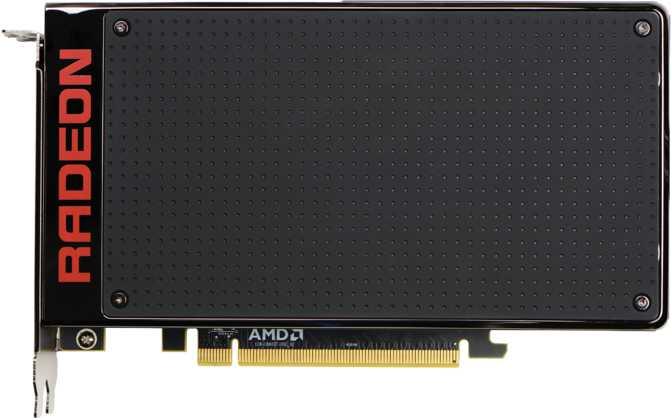
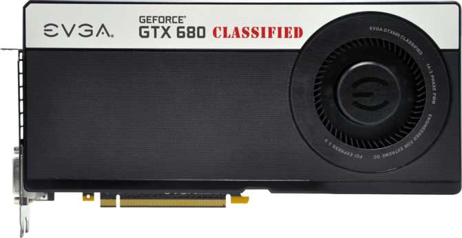
AMD Radeon R9 Fury X vs EVGA GeForce GTX 680 Classified LE
VS
AMD Radeon R9 Fury X

EVGA GeForce GTX 680 Classified LE

AMD Radeon R9 Fury X
EVGA GeForce GTX 680 Classified LE
|
|
AMD Radeon R9 Fury X | EVGA GeForce GTX 680 Classified LE |
|---|---|---|
| GPU Base Clock Speed | 1050MHz | 1006MHz |
| GPU Boost Clock Speed | Not Known | 1058MHz |
| Pixel Rate | 67.2 GPixel/s | 32.2 GPixel/s |
| GPU Memory Speed | 500MHz | 1502MHz |
| GPU Render Output Units (ROPs) | 64 | 32 |
| No. of Supported Displays | 6 | 4 |
|
|
AMD Radeon R9 Fury X | EVGA GeForce GTX 680 Classified LE |
|---|---|---|
| GPU Base Clock Speed | 1050MHz | 1006MHz |
| Pixel Rate | 67.2 GPixel/s | 32.2 GPixel/s |
| FLOPS (Floating-point Performance) | 8.6 TFLOPS | 3.09 TFLOPS |
| Texture Filter Rate | 269 GTexels/s | 129 GTexels/s |
| GPU Memory Speed | 500MHz | 1502MHz |
| Total GPU Shading Units | 4096 | 1536 |
| Total GPU TMUs | 256 | 128 |
| GPU Render Output Units (ROPs) | 64 | 32 |
| DPFP (Double Precision Floating Point) Support |  Yes Yes
|
 Yes Yes
|
| GPU Boost Clock Speed | Not Known | 1058MHz |
|
|
AMD Radeon R9 Fury X | EVGA GeForce GTX 680 Classified LE |
|---|---|---|
| DirectX Version Info | 12 | 11 |
| OpenGL Driver Version | 4.5 | 4.3 |
| OpenCL Driver Version | 2 | 1.1 |
| Multi-display Tech Support |  Yes Yes
|
 Yes Yes
|
| PassMark (G3D) Score | 8191 | 5683 |
| 3DMark Vantage Texture Fill Result | 229.9GTexels/s | 102.04GTexels/s |
| GPU Temperature Under Load | 65°C | 78°C |
| 3DMark Vantage Pixel Fill Result | 40.2GPixel/s | 13.03GPixel/s |
| Idle GPU Temperature | 27°C | 32°C |
| 3D Support |  Yes Yes
|
 Yes Yes
|
| Noise Level Under Load | 43dB | 51.9dB |
| Idle Noise Level | 41.5dB | 40.5dB |
| PassMark (DirectCompute) Benchmark Result | Not Known | 2910 |
| Ray Tracing Support |  No No
|
 No No
|
| Power Consumption Under Peak Load | Not Known | 362W |
| Idle Power Consumption | 82W | 112W |
| Multi-GPU Support Count | 4 | 3 |
| SmallLuxGPU (2.0d4) Result | Not Known | 7800 |
| No. of Supported Displays | 6 | 4 |
|
|
AMD Radeon R9 Fury X | EVGA GeForce GTX 680 Classified LE |
|---|---|---|
| HDMI Output Support |  Yes Yes
|
 Yes Yes
|
| DisplayPort Output | 3 | 1 |
| DVI Output Ports | 0 | 2 |
| Mini DisplayPort Output | 0 | 0 |
|
|
AMD Radeon R9 Fury X | EVGA GeForce GTX 680 Classified LE |
|---|---|---|
| TDP (Thermal Design Point) | No Data Found | No Data Found |
| Transistor Count | 8900 million | 3540 million |
| Semiconductor Size | 28nm | 28nm |
| PCI Express Version | 3 | 3 |
| Air-water Cooling Support |  Yes Yes
|
 No No
|
| Width Size | 191mm | 267mm |
| Dual-GPU Support |  No No
|
 No No
|
| Height | Not Known | 112mm |
|
|
AMD Radeon R9 Fury X | EVGA GeForce GTX 680 Classified LE |
|---|---|---|
| Effective Memory Clock | 1000MHz | 6008MHz |
| Max Memory Bandwidth | 512GB/s | 192GB/s |
| RAM | 4GB | 4GB |
| Memory Bus Interface Width | 4096bit | 256bit |
| GDDR Memory Version | Not Known | 5 |
| ECC (Error-Correcting Code) Memory Support |  No No
|
 No No
|
Similar Comparisons