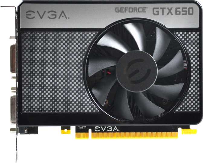
MSI GeForce RTX 3090 Ventus 3X vs EVGA GeForce GTX 650
VS
MSI GeForce RTX 3090 Ventus 3X

EVGA GeForce GTX 650

MSI GeForce RTX 3090 Ventus 3X
EVGA GeForce GTX 650
|
|
MSI GeForce RTX 3090 Ventus 3X | EVGA GeForce GTX 650 |
|---|---|---|
| GPU Base Clock Speed | 1395MHz | 1058MHz |
| GPU Boost Clock Speed | 1695MHz | Not Known |
| Pixel Rate | 189.8 GPixel/s | 8.46 GPixel/s |
| GPU Memory Speed | 1219MHz | 1250MHz |
| GPU Render Output Units (ROPs) | 112 | 16 |
| No. of Supported Displays | 4 | 4 |
|
|
MSI GeForce RTX 3090 Ventus 3X | EVGA GeForce GTX 650 |
|---|---|---|
| GPU Base Clock Speed | 1395MHz | 1058MHz |
| Pixel Rate | 189.8 GPixel/s | 8.46 GPixel/s |
| FLOPS (Floating-point Performance) | 35.58 TFLOPS | 0.81 TFLOPS |
| GPU Memory Speed | 1219MHz | 1250MHz |
| Texture Filter Rate | 556 GTexels/s | 33.9 GTexels/s |
| Total GPU Shading Units | 10496 | 384 |
| Total GPU TMUs | 328 | 32 |
| GPU Boost Clock Speed | 1695MHz | Not Known |
| GPU Render Output Units (ROPs) | 112 | 16 |
| DPFP (Double Precision Floating Point) Support |  No No
|
 Yes Yes
|
|
|
MSI GeForce RTX 3090 Ventus 3X | EVGA GeForce GTX 650 |
|---|---|---|
| DirectX Version Info | 12 | 11 |
| OpenGL Driver Version | 4.6 | 4.3 |
| OpenCL Driver Version | 2 | 1.1 |
| Multi-display Tech Support |  Yes Yes
|
 Yes Yes
|
| 3D Support |  Yes Yes
|
 Yes Yes
|
| No. of Supported Displays | 4 | 4 |
| PassMark (G3D) Score | Not Known | 1825 |
| 3DMark Vantage Texture Fill Result | Not Known | 26.4GTexels/s |
| GPU Temperature Under Load | Not Known | 51°C |
| 3DMark Vantage Pixel Fill Result | Not Known | 3.8GPixel/s |
| PassMark (DirectCompute) Benchmark Result | Not Known | 825 |
| Ray Tracing Support |  Yes Yes
|
 No No
|
| Idle GPU Temperature | Not Known | 27°C |
| Noise Level Under Load | Not Known | 43.5dB |
| Power Consumption Under Peak Load | Not Known | 231W |
| Idle Power Consumption | Not Known | 104W |
| Idle Noise Level | Not Known | 43dB |
| SmallLuxGPU (2.0d4) Result | Not Known | 2100 |
|
|
MSI GeForce RTX 3090 Ventus 3X | EVGA GeForce GTX 650 |
|---|---|---|
| HDMI Output Support |  Yes Yes
|
 Yes Yes
|
| GPU HDMI Version | 2.1 | Not Known |
| DisplayPort Output | 3 | 0 |
| No. of HDMI Ports | 1 | Not Known |
| DVI Output Ports | 0 | 2 |
| Mini DisplayPort Output | 0 | 1 |
|
|
MSI GeForce RTX 3090 Ventus 3X | EVGA GeForce GTX 650 |
|---|---|---|
| TDP (Thermal Design Point) | No Data Found | No Data Found |
| Transistor Count | 28300 million | 1270 million |
| Semiconductor Size | 8nm | 28nm |
| PCI Express Version | 4 | 3 |
| Dual-GPU Support |  No No
|
 No No
|
| Air-water Cooling Support |  No No
|
 No No
|
| Width Size | 305mm | 152mm |
| Height | 120mm | 111mm |
|
|
MSI GeForce RTX 3090 Ventus 3X | EVGA GeForce GTX 650 |
|---|---|---|
| Effective Memory Clock | 19500MHz | 5000MHz |
| Max Memory Bandwidth | 936GB/s | 80GB/s |
| RAM | 24GB | 1GB |
| Memory Bus Interface Width | 384bit | 128bit |
| GDDR Memory Version | 6 | 5 |
| ECC (Error-Correcting Code) Memory Support |  No No
|
 No No
|
Similar Comparisons